-
价格公道
价格公道
-
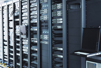
服务
买的开心,用的放心
-
只做正品
原厂原装、现货库存
-
专营存储芯片10年以上
有丰富的服务和供货经验
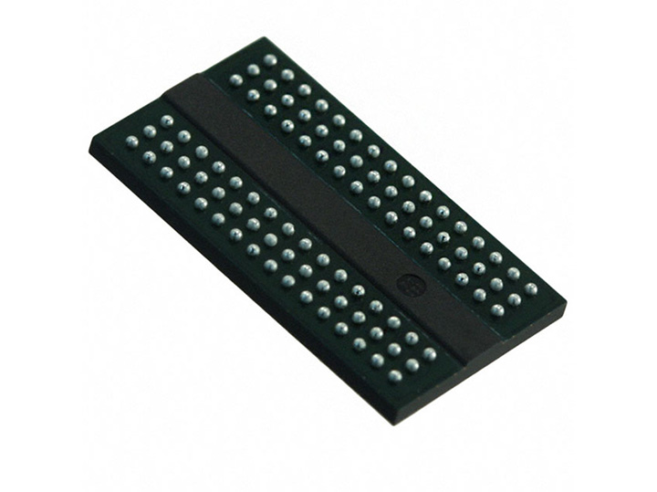
品牌:SK hynix/海力士
型号:H5TQ2G63FFR-PBC
容量:2GBIT
技术:DDR3 SDARM
H5TQ2G63FFR-PBC产品信息:
品牌:SK hynix/海力士
型号:H5TQ2G63FFR-PBC
容量:2GBIT
技术:DDR3 SDARM
产品族:存储器
类别:集成电路IC
格式:闪存
电压:1.35V/1.5V
Speed:N1C/N0C/11C
封装:96FBGA
H5TC(Q)2G63FFR:
The H5TC(Q)2G63FFR-xxC are a 2,147,483,648-bit CMOS Double Data Rate III (DDR3) Synchronous DRAM, ideally suited for the graphics applications which require large memory density and high bandwidth and low power operation. 1.35v speed part provides backward compatibility with 1.5V DDR3. SK hynix 2Gb DDR3 SDRAM offer fully synchronous operations referenced to both rising and falling edges of the clock. While all addresses and control inputs are latched on the rising edges of the CK (falling edges of the CK), Data, Data strobes and Write data masks inputs are sampled on both rising and falling edges of it. The data paths are internally pipelined and 8-bit prefetched to achieve very high bandwidth.
Features:
DQ Power & Power supply:
VDD=VDDQ=1.35V + 0.100 / - 0.065V
VDD=VDDQ=1.5V +/- 0.075V
Fully differential clock inputs (CK, CK) operation
Differential Data Strobe (DQS, DQS)
On chip DLL align DQ, DQS and DQS transition with CK transition
DM masks write data-in at the both rising and falling edges of the data strobe
All addresses and control inputs except data, data strobes and data masks latched on the rising edges of the clock
Programmable CAS latency 5, 6, 7, 8, 9, 10,11,12,13,14 and 15 supported
Programmable additive latency 0, CL-1, and CL-2 supported
Programmable CAS Write latency (CWL) = 5, 6, 7, 8, 9, 10 and 11
Programmable burst length 4/8 with both nibble
sequential and interleave mode
BL switch on the fly
8banks
8K refresh cycle/64ms
Auto Self Refresh supported
JEDEC standard 96ball FBGA (x16)
Driver strength selected by EMRS
Dynamic On Die Termination supported
Asynchronous RESET pin supported
ZQ calibration supported
Write Levelization supported
8 bit pre-fetch
描述:H5TQ2G63FFR-PBC IC FLASH 存储器 DDR3 SDARM 2GBIT 96FBGA
电话:0755-82216365
手机:159-9967-6523
传真:0755-82787199
邮箱:sales@gayocen.cn
QQ:3007317879
地址:广东省深圳市福田区华强北路华强广场A座10I

扫码关注我们
Copyright © 2020 深圳市广运诚科技有限公司版权所有 粤ICP备20038713号